


PCB Solder Joint Fillet - Guide to Quality and Defects
Author Dmitrii KhramtsovPosted 14 June 2026
Updated 14 June 2026

What is a solder joint fillet?
It is the shape of the solder between the contact pad, the component lead, and the solder joint itself. The formation of the correct shape depends on sufficient heating temperature of the entire joint, including the printed circuit board. It also depends on the flux, which helps the molten solder flow freely. And due to the cApillary effect form a smooth concave fillet shape.
Why does the fillet shape matter?
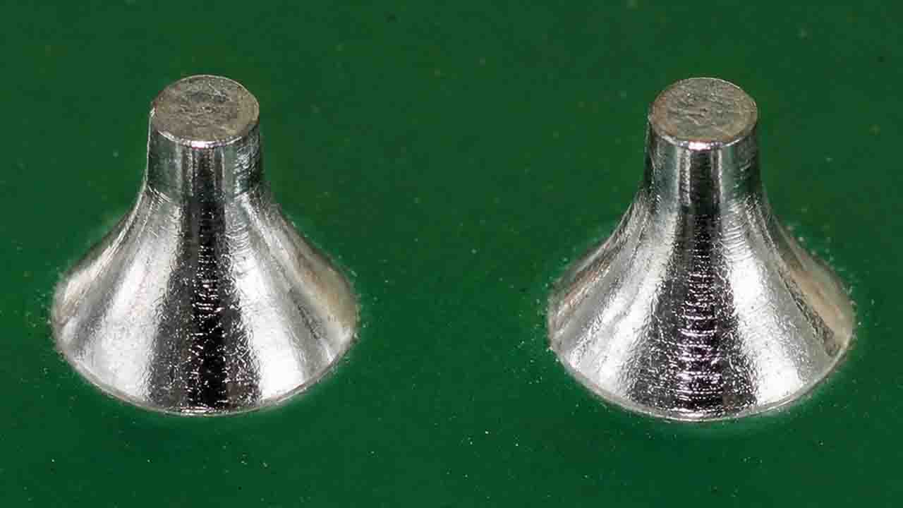
The fillet shows the level of wetting, the quality of the solder contact with the metal, and indirectly tells us - how correctly the metallurgical bond between the solder, the pcb pad, and the component lead was formed. It also tells us whether there were problems with temperature and cleanliness of the solder joints during reflow. A good fillet should not look like a drop placed on top of the contact. It should have a smooth transition from the pad to the lead.
A sharp angle, a spherical shape, or solder that stands like a “hill” often indicates poor wetting and bad soldering.
Let’s take a look at these Solder Joint defects!
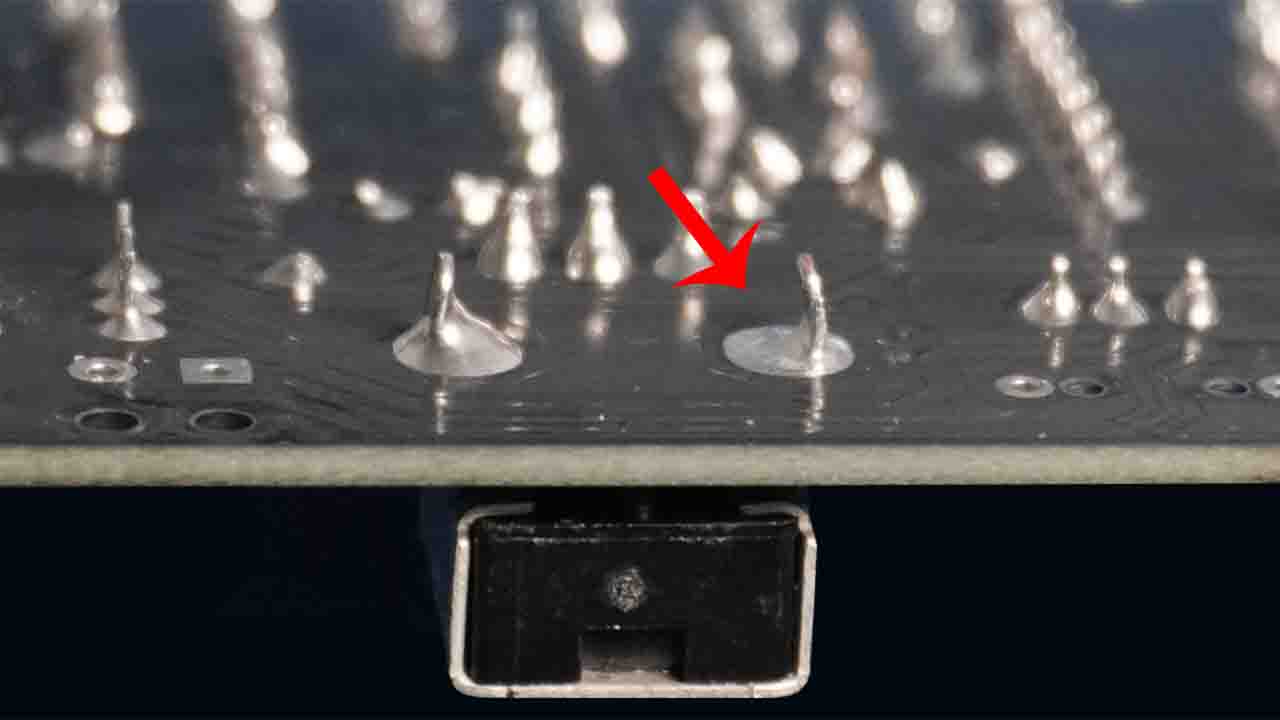
Too little solder on the pad.
This is the first indicator that the soldering process was violated. The joint may be stable, but its mechanical strength will not allow us to guarantee long-term reliability. With a small fillet, we can understand that the solder joint is not fixed along the full height of the component. The height and width of the fillet should be approximately the same, depending from component height. Even if there is good solder fill inside the plated hole for the component lead, a small fillet on top is still a defect according to IPC standards.
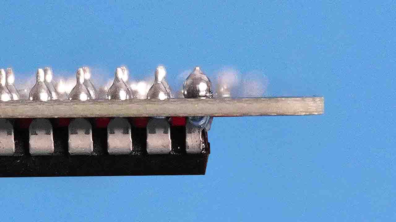
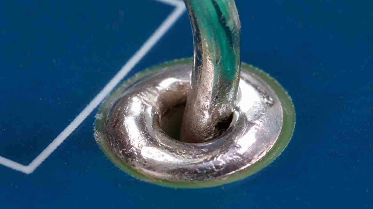
Too much solder.
Many people think that the more solder there is, the more reliable the joint is — this is not true. Excess solder on top in the form of a ball, a sharp peak, a needle, a solder protrusion, or an extension, is always bad and is considered a defect according to the IPC-A-610 standard.
Too much solder on top may indicates that during solder formation, the alloy did not have enough fluidity because of low temperature, insufficient flux, or poor-quality flux. There is a high probability that the contact of the alloy with the PCB pad and inside the plated hole is also poor. Or it could also indicate a solder paste stencil that is too thick, or sloppy manual soldering. All defects have a cause.
If poor wetting is visible from the outside, then inside the joint there will also be poor wetting, a weak metallurgical bond, and unreliable contact.
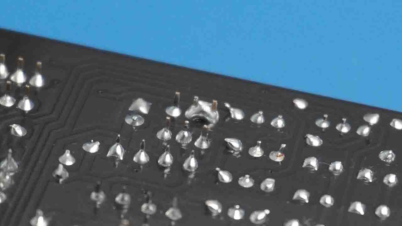
Solder bridges between joints.
This is an obvious defect. Excess solder can form bridges between joints. This short circuit between leads can lead to damage to some components. Bridges can be barely visible, especially when components and leads are located very densely on the printed circuit board.
If you design printed circuit boards yourself, be sure to consider the size of the contact pads and the distance between them, according with IPC standards.
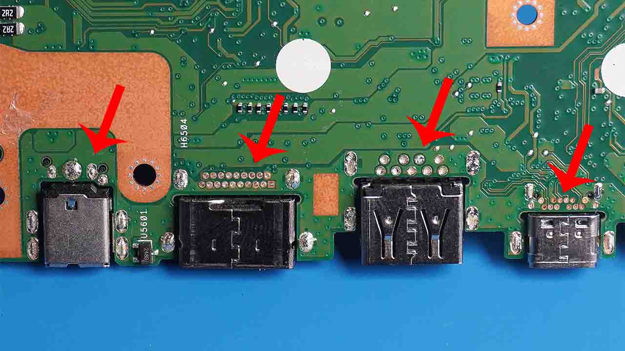
Insufficient solder fill in plated holes.
Carefully inspect both sides of one lead.
If this is a component lead passing through a plated hole, then the fillet on both sides must have the correct shape. This tells us that the hole is fully filled with solder, and the solder has formed a joint with the hole plating.
If this is a connector lead that, by design, does not come out on the back side of the board, then it is enough for us to see, that the hole is filled with solder. And that a normal fillet has formed on the connector side with a reliable joint between the solder, the lead, and the hole plating.
A very important detail — the lead is cut at the top of the soldered joint, and after that, this lead must be solder again to tin the exposed cut metal of the lead. Otherwise, you risk seeing rust on the cut section. More about this in my video about pcb rust — the link is in the description.
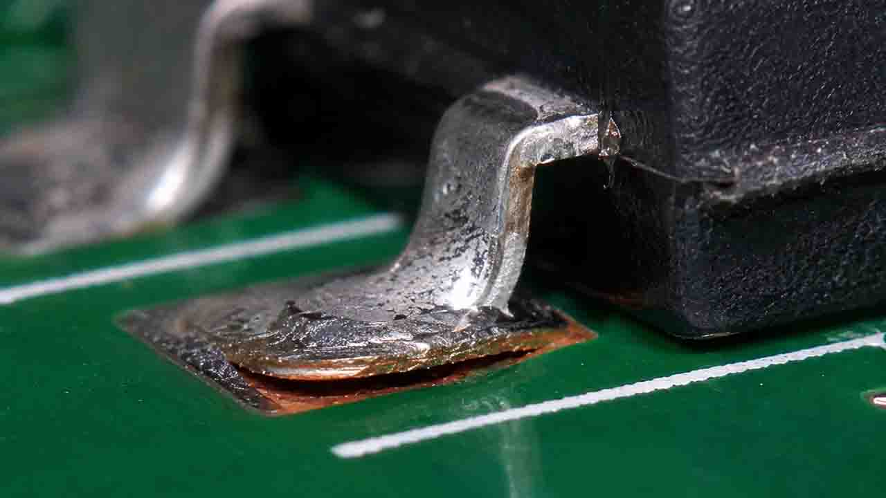
Torn fillet edges due to delamination on the pad or component.
The quality of the joint between the solder, the PCB pad, and the component, tells us about surface contamination, the presence of oxides, or delamination. This is a 100% defect according to IPC and cannot be considered a reliable joint.
The soldered surfaces must be clean — without obvious oxide spots, without delamination, and degreased. In one word — clean. Otherwise, there is a high probability that the joint will not withstand dynamic load during device operation, and the solder joint could come loose.
If there is no way to properly restore the PCB contact pad, always use fixing adhesives for the component. And if the surface of the component itself is bad, it is better to buy a new one.
Visible base metal of the contact pad after soldering.
This is also a defect according to IPC. Visible base metal areas of the contact pad after soldering tell us either about insufficient wettability of the surface by the flux, or about contamination on the contact pad. The solder must fully cover the required soldering area of the contact pad without exposed areas. Maybe a little bit on the edge of the pad.
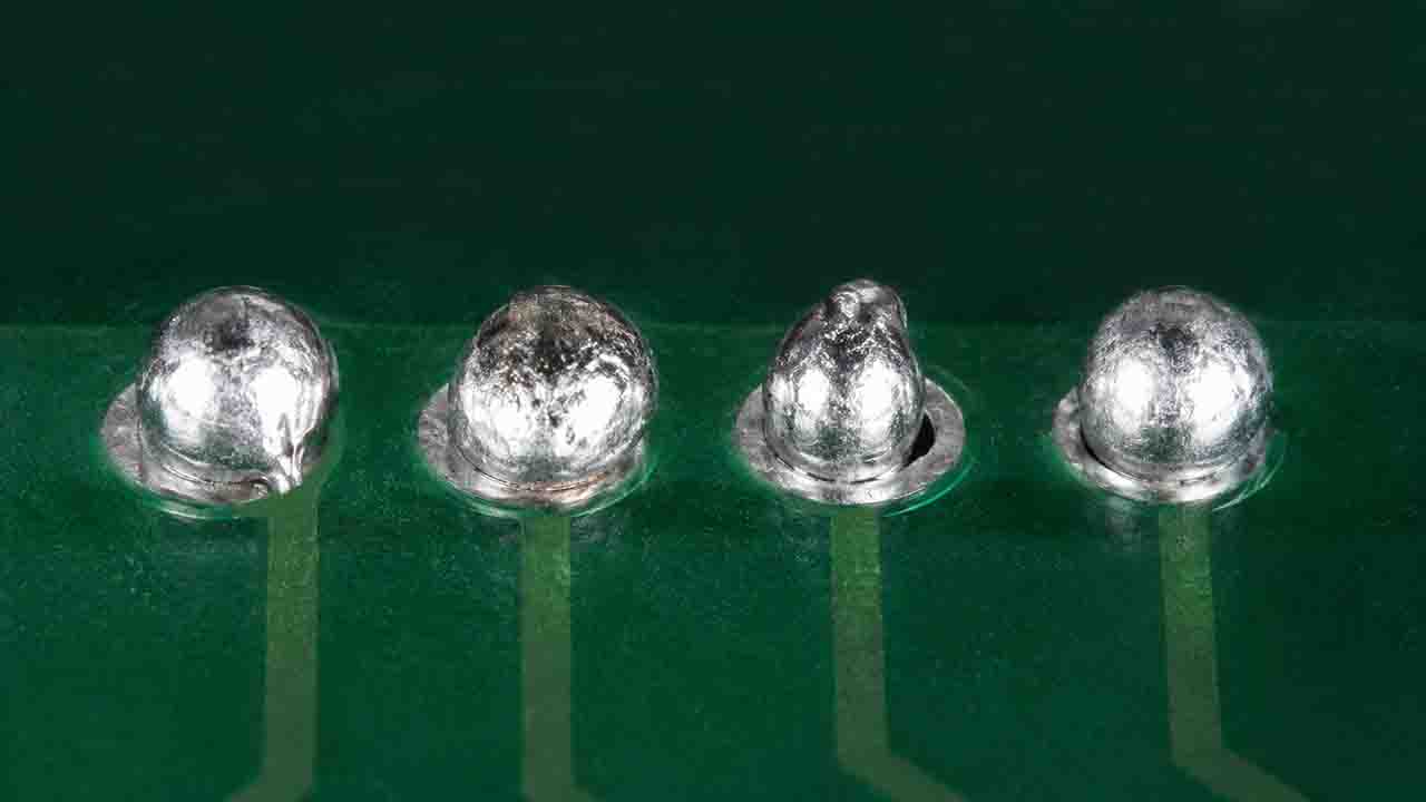
Cold solder joint.
From the definition itself, it follows that during solder reflow, the temperature was insufficient. A cold solder joint may look normal, but with careful inspection under a microscope, you can notice a gap between the contact pad and the solder, or between the component lead and the solder.
Three bodies participate in the creation of a solder joint — the printed circuit board, the component, and the solder. The printed circuit board is most often the body with the highest thermal mass.
Therefore, for regular soldering, I recommend using the correct soldering iron tip temperatures — 320 degrees Celsius for lead alloys and 350 degrees Celsius for lead-free alloys. Use a regular 2 mm wave tip.
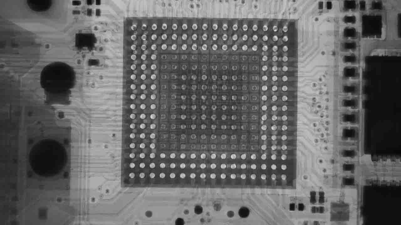
Hidden defects.
The external appearance cannot always honestly tell us about the quality of all connections inside. I first evaluate the outside. A good microscope is needed. It is necessary to inspect the joints from different angles to make sure that all fillets are correctly formed, that all joints are soldered, and that they have the correct fillet shapes.
When through-hole leads are present, we must always look at the back side of the printed circuit board — the solder must be visible. But the presence of solder alone is not enough. It must not simply fill the hole like a plug. The solder must be joined to the walls of the plated hole and to the contact pad on the surface of the printed circuit board.
For joints under microcircuits, the most reliable inspection method is X-ray. X-ray inspection is only used in manufacturing. In our conditions, we can use only soldering technology, microscopes, correct temperatures, high-quality solders and solder pastes, fluxes, and clean surfaces.
Thank you for reading!
Watch video PCB Solder Joints