


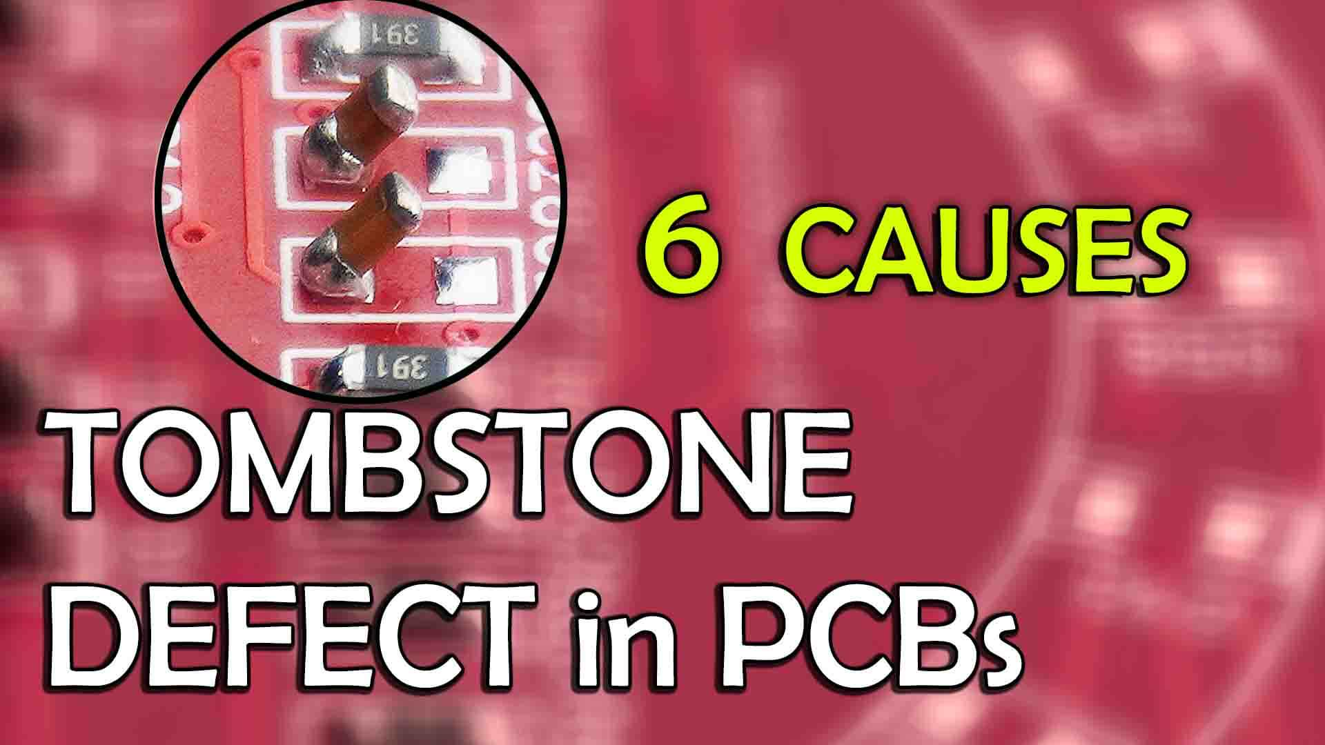
Tombstone Effect with SMD in Electronic PCB
Author: Khramtsov DmitriiPosted: 2 April 2025
Updated: 2 April 2025
Introduction
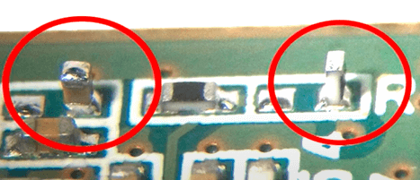
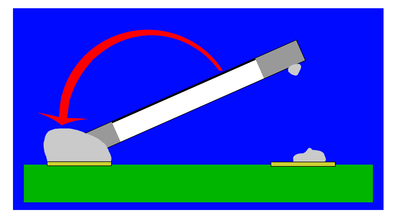
Hello! My name is Dmitrii. In this article, I’ll explain the “Tombstone Effect”, also known as the Manhattan effect, chip lifting, Stonehenge effect, or drawbridge effect. That effect occurs during the reflow process of solder paste on a PCB in an oven. With this effect, an SMD component – a resistor, capacitor, or any other - lifts on one contact pad and detaches from the other pad. I’ll tell you six causes of this defect and how to prevent it.
1 – Incorrect Reflow Profile Creating Temperature Differences on the Two Pads.
In the reflow oven, different profiles are used for leaded and lead-free solder pastes. In one of my upcoming videos, I’ll show you how to build a reflow profile. In this case, the conveyor speed is too high, and the PCB does not spend enough time in the oven’s second zone to stabilize its temperature. You need to align the profile with the solder paste manufacturer’s recommendations. Then test the actual temperatures in the oven zones using a thermal profiler. The correct profile will preheat the PCB and components evenly by the time the solder paste melts.
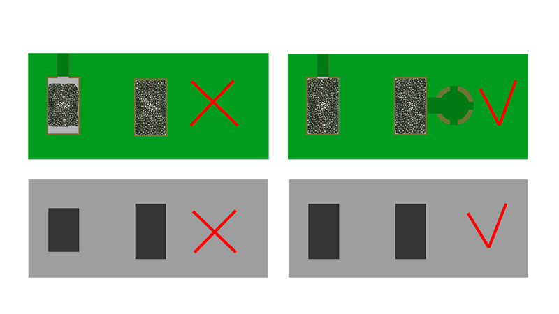
2 – Lack of a Thermal Barrier on One of the Pads.
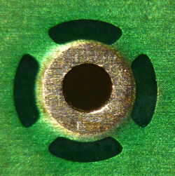
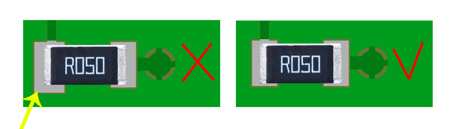
3 – A Via Hole Located on One of the Pads.
When a via is placed on one of the contact pads, heat leaks into the metallized through hole, disrupting uniform heating. When designing, place vias outside the pads and provide thermal relief. Additionally, solder may leak into the via, shifting the surface tension difference to the other pad, which then pulls the component toward it. The solution is to redesign the PCB.
4 – Different volumes of solder paste on two pads.
5 – Different sized pads on either side of a symmetrical component.
6 – A Poorly Made Stencil That Clogs with Solder Paste.
Conclusion
In Conclusion… by making PCB corrections at the planning stage, you can eliminate future PCB soldering issues, avoid costly repairs, and significantly improve the quality of your PCBs. Be sure to check out my other videos on the channel to further improve your skills.
Thank you for reading!
Watch video about Tombstone Effect / Defect in Electronics