


Tenting Vias in Electronic PCB Design to Prevent Soldering Issues
Author Dmitrii KhramtsovPosted 09 July 2025
Updated 09 July 2025
The PCBs was soldered at the manufactory, tested, and sent to the customer — and a few months later, the customer comes back with a problem: the PCBs stop functioning properly. In this article, I’ll explain why it’s very important to cover vias with solder mask.
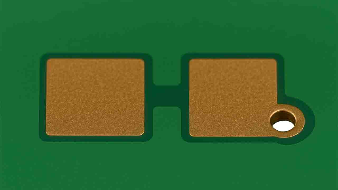
A via is used to connect traces between layers of a PCB.
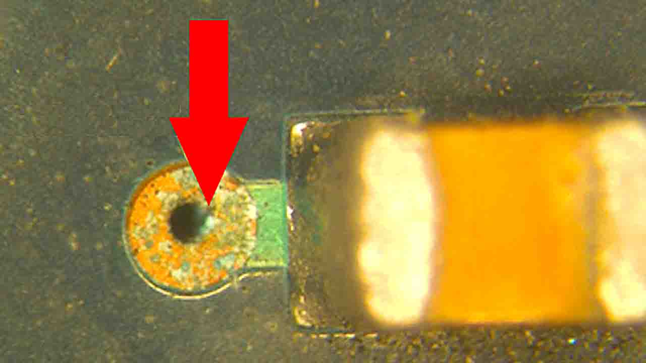
Molten solder flowing from a pad into an open via.
One of the biggest design mistakes is placing a via inside a pad for soldering.
During soldering or reflowing solder paste, the molten alloy flows into the via. This causes defects — not enough solder on one side of the SMD component, which often results in the tombstone effect.
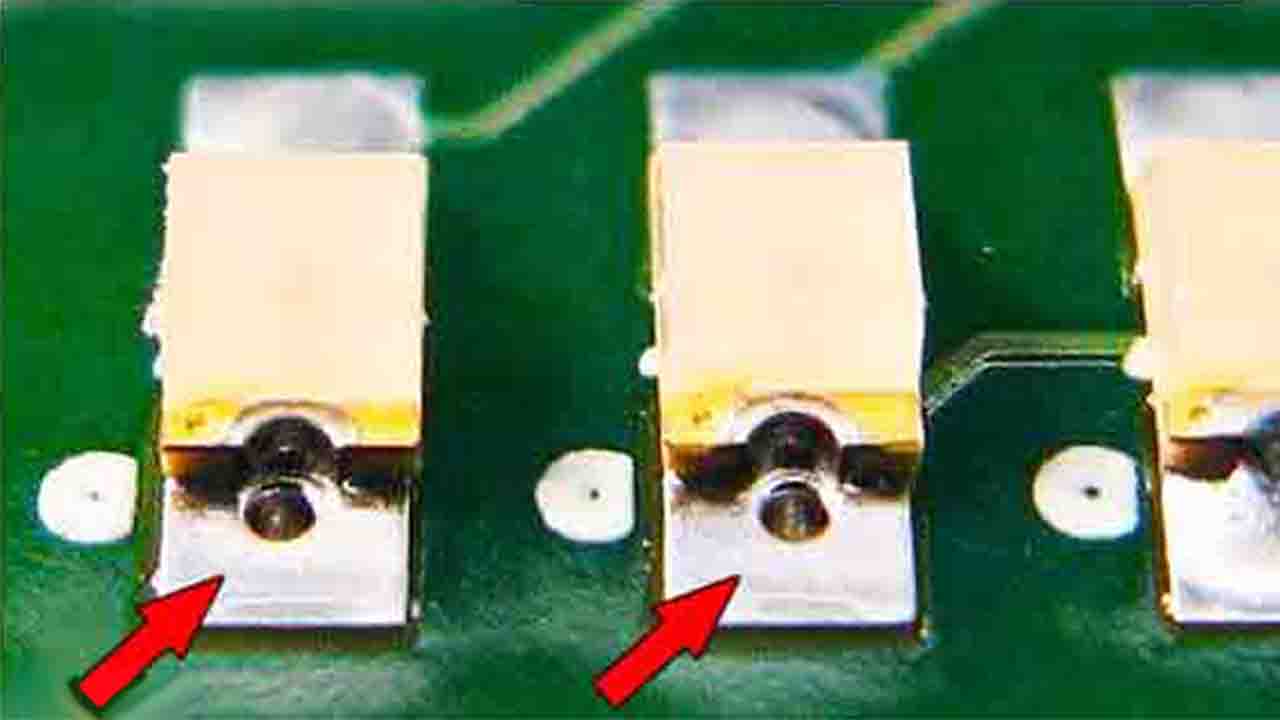
Too little solder alloy on one side of the component will lead to cracks from vibration, and the component loses a reliable connection. Of course, this kind of PCB will have to be manually reworked to add the missing solder to the component leads. That’s all added cost.
If open vias are located under a BGA, this can become a major problem if solder flows from the BGA ball joint into the via.
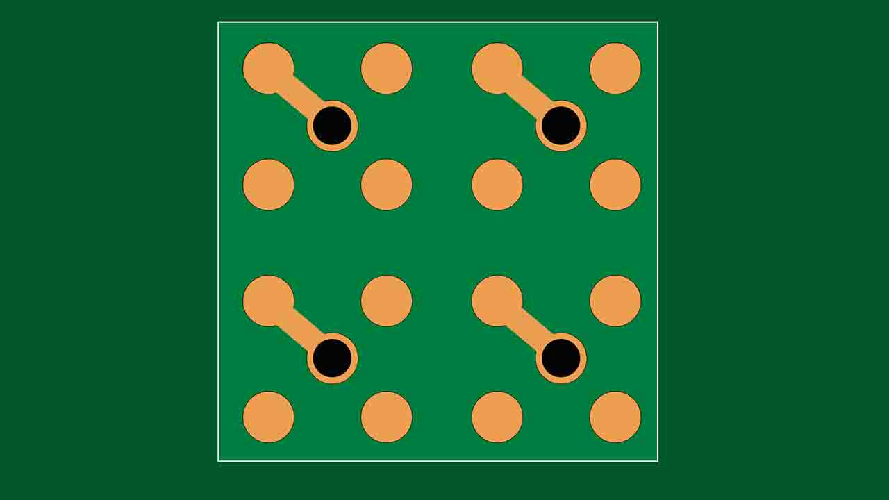
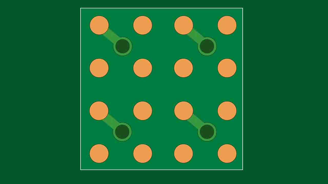
The vias should be moved outside the pads and covered with solder mask on both sides of the PCB. If the vias is large enough, PCB manufacturers use different resins to fill the vias and then apply the mask on top. You need to take this into account when ordering PCBs. How often you run into mistakes like this?
Soldering Flux and moisture flowing into open vias
Soldering Fluxes vary, but even residues from no-clean flux can absorb moisture over time, especially when the device operates in a humid environment. Even without flux, a empty vias is still subject to moisture exposure. Moisture triggers oxidation and corrosion inside the vias. In this case, the copper inside the vias will eventually rot, and the PCB will stop functioning properly.
Now imagine a PCB assembling manufactory using cheap Chinese solder paste with unknown flux inside! If the flux is active, its residues in the vias will quickly trigger corrosion, and the copper in the vias will oxidize.
If you soldering PCBs using wave soldering technology, then vias tenting becomes especially important. Always take this into account when designing electronics PCBs — this is called via tenting. Do you use via tenting in your projects, or do you think it’s unnecessary?
I provide consulting services for electronics manufacturers, help with PCB defect analysis and soldering issues in production.
Thank you for reading!
Watch video Via Tenting in Electronic PCB!