


PCB Panelization: V-SCORING or TAB-ROUTING
Author Dmitrii KhramtsovPosted 12 September 2025
Updated 12 September 2025
Have you ever wondered why blank PCBs are often manufactured in one large panels of several PCBs? And how are these panels then separated?
If the design of the connection of PCBs into one large blank panel is incorrect, and when separating it, it’s easy to damage the components, installed on the edges of the PCBs or damage copper tracks. Let's figure it out!
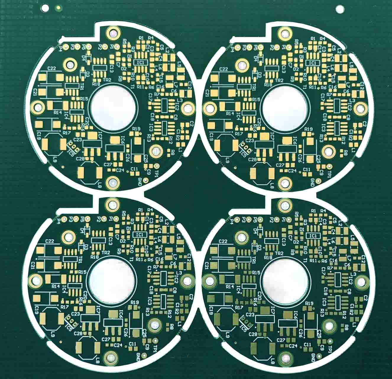
For convenience and speed up of assembly and soldering, PCBs are combined into panel of several PCBs. PCBs may be similar, may be different in 1 panel. This can be 1 panel with 4 large Printed Circuit Boards or a panel with 24 small PCBs.
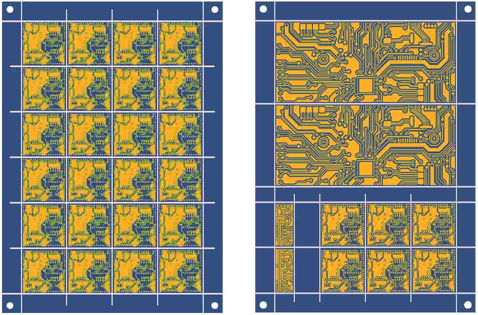
After assembling and soldering, these PCBs must be separated from each other and there are several methods. I will tell you about two most popular.
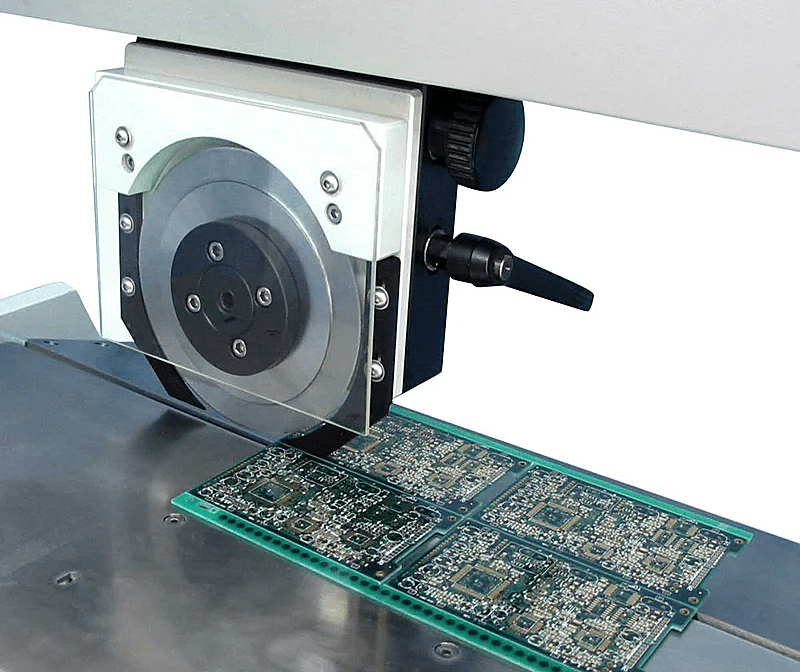
V-scoring PCB separation
This method of separation is used in cases, where the printed circuit board has a square or rectangular shape without rounding’s. V-shaped grooves are cut along the lines of the future separation on both sides of the PCBs.
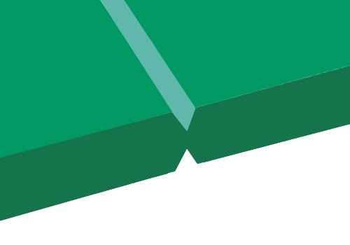
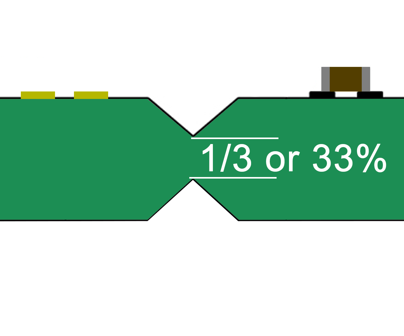
In the places of the V-shaped grooves, the thickness of the PCB remains 33% of the total thickness. This is enough for the rigidity of the panel when placing electronic components, reflow and ease of separation at the finish of the assembly cycle.
It would seem to be a simple cut, but this is exactly what greatly speeds up the process of PCBs assembling circle.
PCB separator with roller knives, rolling along V-cuts. Most often used for separation in PCB assembling manufactory.
Fast method, neat edge, suitable for large batches of Printed circuit boards.
Works only for straight lines. When splitting, non-critical mechanical stresses are created, so components and copper tracks should be spaced at least 3 mm from the edge.
PCB Milling with holes in jumpers.
The contours of all PCBs in one panel are cut with a milling cutter. To hold all PCBs in one panel, small jumpers with small holes are left. This method is used for PCBs of complex shapes, with curved lines and internal cutouts.
Such a panel must be separated by carefully breaking the jumpers with mouse bites using pliers or another tool, holding the board and bending it. If necessary, jumpers and burrs can be cleaned with a file for metal or emery stone.
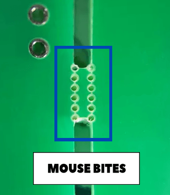
If remains of jumpers don’t interfere, you can leave them. But, look at remains of jumpers on the edge - these remains can be a real nightmare for the aesthetics of PCB.
In my work I separated such PCBs with pliers and side cutters. The method works, although it looks ugly. Therefore, a file for metal or emery stone are your best friends.
Pros - allows you to combine printed circuit boards of any shape into a panel. The panel remains strong and does not deform.
Cons: after separation, remains must be manually cleaned.
Important rule when PCB designing
A key point that even experienced engineers forget. If components are too close to the edge of the PCB, then get ready for problems!
Don’t place components and copper tracks close to the edge of the PCB. The minimum distance is 3 mm from the separation line.
Why?
- 1. There is a high probability of damaging the conductors and risk of damaging soldered components when separating.
- 2. You can tear out the pads with SMD components when separating.
- 3. When placing components on Pick & Place machine, the edge components pads may be hidden behind the conveyor clamp and then you will have to soldering the edge components manually.
Before ordering PCBs in panels, be sure which method of PCB panelization you want to use for separation:
V-scoring or PCB Milling.
It would seem that this is a simple article, but that's exactly why companies lose thousands of dollars on defects, damaging PCB boards and manual PCB repairing.
Thank you for reading!
Watch video PCB Panelization: V-SCORING or TAB-ROUTING